- 您现在的位置:买卖IC网 > Sheet目录2000 > IDT5T9890NLI8 (IDT, Integrated Device Technology Inc)IC CLK DRIVER 2.5V PLL 68-VFQFPN
18
INDUSTRIALTEMPERATURERANGE
IDT5T9890
EEPROM PROGRAMMABLE 2.5V PROGRAMMABLE SKEW PLL CLOCK DRIVER
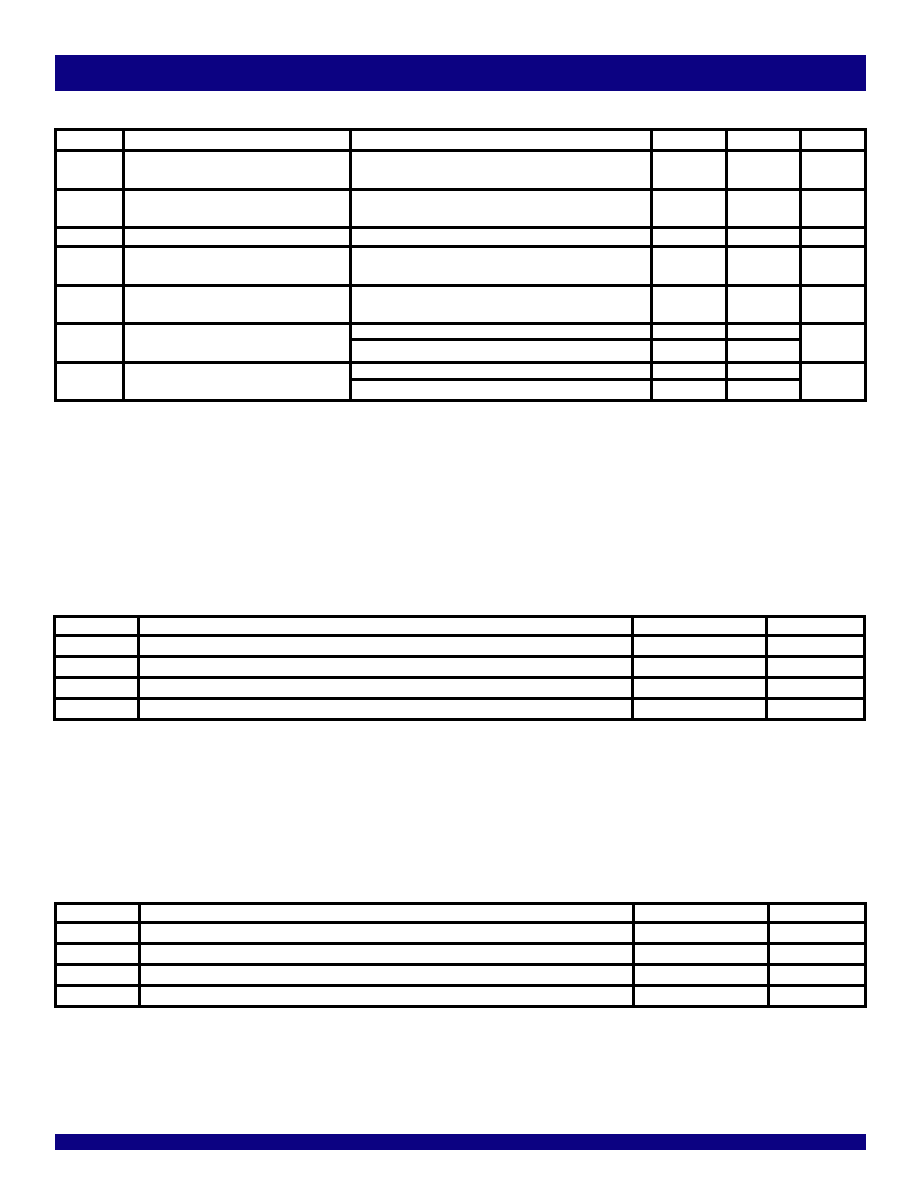
SINGLE-ENDED INPUT AC TEST CONDITIONS FOR 1.8V LVTTL
Symbol
Parameter
Value
Units
VIH
Input HIGH Voltage(1)
VDDI
V
VIL
InputLOWVoltage
0V
VTHI
InputTimingMeasurementReferenceLevel(2)
VDDI/2
mV
tR, tF
InputSignalEdgeRate(3)
2
V/ns
NOTES:
1. VDDI is the nominal 1.8V supply (1.8V ± 0.15V) of the part or source driving the input.
2. A nominal 900mV timing measurement reference level is specified to allow constant, repeatable results in an automatic test equipment (ATE) environment.
3. The input signal edge rate of 2V/ns or greater is to be maintained in the 10% to 90% range of the input waveform.
DIFFERENTIAL INPUT AC TEST CONDITIONS FOR 1.8V LVTTL
Symbol
Parameter
Value
Units
VDIF
Input Signal Swing(1)
VDDI
V
VX
DifferentialInputSignalCrossingPoint(2)
VDDI/2
mV
VTHI
InputTimingMeasurementReferenceLevel(3)
CrossingPoint
V
tR, tF
InputSignalEdgeRate(4)
1.8
V/ns
NOTES:
1. VDDI is the nominal 1.8V supply (1.8V ± 0.15V) of the part or source driving the input. A nominal 1.8V peak-to-peak input pulse level is specified to allow consistent, repeatable
results in an automatic test equipment (ATE) environment. This device meets the VDIF (AC) specification under actual use conditions.
2. A nominal 900mV crossing point level is specified to allow consistent, repeatable results in an automatic test equipment (ATE) environment. This device meets the VX specification
under actual use conditions.
3. In all cases, input waveform timing is marked at the differential cross-point of the input signals.
4. The input signal edge rate of 1.8V/ns or greater is to be maintained in the 20% to 80% range of the input waveform.
NOTES:
1. These power consumption characteristics are for all the valid input interfaces and cover the worst case input and output interface combinations.
2. The termination resistors are excluded from these measurements.
3. If the differential input interface is used, the true input is held LOW and the complementary input is held HIGH.
4. Bit 60 = 1.
5. All outputs are at the same interface level.
POWER SUPPLY CHARACTERISTICS FOR 1.8V LVTTL OUTPUTS(1)
Symbol
Parameter
Test Conditions(2)
Typ.
Max
Unit
IDDQ
Quiescent VDD Power Supply Current(3)
VDDQN = Max., REF = LOW, PD = HIGH, nSOE = LOW,
112
150
mA
PLL_EN = HIGH, Outputs enabled, All outputs unloaded
IDDQQ
Quiescent VDDQN Power Supply Current(3)
VDDQN = Max., REF = LOW, PD = HIGH, nSOE = LOW,
3
75
A
PLL_EN = HIGH, Outputs enabled, All outputs unloaded
IDDPD
Power Down Current
VDD = Max., PD = LOW, nSOE = LOW, PLL_EN = HIGH
0.7
3
mA
IDDD
Dynamic VDD Power Supply
VDD = Max., VDDQN = Max., CL = 0pF
18
30
A/MHz
CurrentperOutput
IDDDQ
Dynamic VDDQN Power Supply
VDD = Max., VDDQN = Max., CL = 0pF
19
30
A/MHz
CurrentperOutput
ITOT
Total Power VDD Supply Current(4,5)
VDDQN = 1.8V., FVCO = 100MHz, CL = 15pF
275
400
mA
VDDQN = 1.8V., FVCO = 250MHz, CL = 15pF
310
450
ITOTQ
Total Power VDDQN Supply Current(4,5)
VDDQN = 1.8V., FVCO = 100MHz, CL = 15pF
135
200
mA
VDDQN = 1.8V., FVCO = 250MHz, CL = 15pF
200
300
发布紧急采购,3分钟左右您将得到回复。
相关PDF资料
IDT5V19EE604NDGI8
IC PLL CLK GEN 200MHZ 28VFQFPN
IDT5V40501DVG
IC CLK GEN PLL 160MHZ 8TSSOP
IDT5V41064NLGI
IC CLK GEN 1:1 16QFN
IDT5V41066PGG
IC CLK GEN SPRED SPECTRM 20TSSOP
IDT5V49EE901NLGI8
IC PLL CLK GEN 200MHZ 32VFQFN
IDT5V49EE902NLGI
IC CLOCK GEN PLL 500MHZ 32VFQFPN
IDT5V49EE904NLGI8
IC PLL CLK GEN 200MHZ 32VFQFN
IDT821024PPG
IC PCM CODEC QUAD NONPROG 44TQFP
相关代理商/技术参数
IDT5T9891NLGI
功能描述:IC CLK DRIVER 2.5V PLL 68-VFQFPN RoHS:是 类别:集成电路 (IC) >> 时钟/计时 - 时钟发生器,PLL,频率合成器 系列:- 标准包装:39 系列:- 类型:* PLL:带旁路 输入:时钟 输出:时钟 电路数:1 比率 - 输入:输出:1:10 差分 - 输入:输出:是/是 频率 - 最大:170MHz 除法器/乘法器:无/无 电源电压:2.375 V ~ 3.465 V 工作温度:0°C ~ 70°C 安装类型:* 封装/外壳:* 供应商设备封装:* 包装:*
IDT5T9891NLGI8
功能描述:IC CLK DRIVER 2.5V PLL 68-VFQFPN RoHS:是 类别:集成电路 (IC) >> 时钟/计时 - 时钟发生器,PLL,频率合成器 系列:- 标准包装:39 系列:- 类型:* PLL:带旁路 输入:时钟 输出:时钟 电路数:1 比率 - 输入:输出:1:10 差分 - 输入:输出:是/是 频率 - 最大:170MHz 除法器/乘法器:无/无 电源电压:2.375 V ~ 3.465 V 工作温度:0°C ~ 70°C 安装类型:* 封装/外壳:* 供应商设备封装:* 包装:*
IDT5T9891NLI
功能描述:IC CLK DRIVER 2.5V PLL 68-VFQFPN RoHS:否 类别:集成电路 (IC) >> 时钟/计时 - 时钟发生器,PLL,频率合成器 系列:- 标准包装:39 系列:- 类型:* PLL:带旁路 输入:时钟 输出:时钟 电路数:1 比率 - 输入:输出:1:10 差分 - 输入:输出:是/是 频率 - 最大:170MHz 除法器/乘法器:无/无 电源电压:2.375 V ~ 3.465 V 工作温度:0°C ~ 70°C 安装类型:* 封装/外壳:* 供应商设备封装:* 包装:*
IDT5T9891NLI8
功能描述:IC CLK DRIVER 2.5V PLL 68-VFQFPN RoHS:否 类别:集成电路 (IC) >> 时钟/计时 - 时钟发生器,PLL,频率合成器 系列:- 标准包装:39 系列:- 类型:* PLL:带旁路 输入:时钟 输出:时钟 电路数:1 比率 - 输入:输出:1:10 差分 - 输入:输出:是/是 频率 - 最大:170MHz 除法器/乘法器:无/无 电源电压:2.375 V ~ 3.465 V 工作温度:0°C ~ 70°C 安装类型:* 封装/外壳:* 供应商设备封装:* 包装:*
IDT5T989X-982X-M1
功能描述:KIT FOR 5T989X-982X RoHS:否 类别:编程器,开发系统 >> 评估演示板和套件 系列:- 标准包装:1 系列:- 主要目的:电信,线路接口单元(LIU) 嵌入式:- 已用 IC / 零件:IDT82V2081 主要属性:T1/J1/E1 LIU 次要属性:- 已供物品:板,电源,线缆,CD 其它名称:82EBV2081
IDT5T9950APFGI
功能描述:IC CLK BUFFER/DVR 1:10 32TQFP RoHS:是 类别:集成电路 (IC) >> 时钟/计时 - 时钟发生器,PLL,频率合成器 系列:TurboClock™ II JR 标准包装:1,000 系列:- 类型:时钟/频率合成器,扇出分配 PLL:- 输入:- 输出:- 电路数:- 比率 - 输入:输出:- 差分 - 输入:输出:- 频率 - 最大:- 除法器/乘法器:- 电源电压:- 工作温度:- 安装类型:表面贴装 封装/外壳:56-VFQFN 裸露焊盘 供应商设备封装:56-VFQFP-EP(8x8) 包装:带卷 (TR) 其它名称:844S012AKI-01LFT
IDT5T9950APFGI8
功能描述:IC CLK BUFFER/DVR 1:10 32TQFP RoHS:是 类别:集成电路 (IC) >> 时钟/计时 - 时钟发生器,PLL,频率合成器 系列:TurboClock™ II JR 标准包装:1,000 系列:- 类型:时钟/频率合成器,扇出分配 PLL:- 输入:- 输出:- 电路数:- 比率 - 输入:输出:- 差分 - 输入:输出:- 频率 - 最大:- 除法器/乘法器:- 电源电压:- 工作温度:- 安装类型:表面贴装 封装/外壳:56-VFQFN 裸露焊盘 供应商设备封装:56-VFQFP-EP(8x8) 包装:带卷 (TR) 其它名称:844S012AKI-01LFT
IDT5T9950PFGI
功能描述:IC CLK BUFFER/DVR 1:10 32TQFP RoHS:是 类别:集成电路 (IC) >> 时钟/计时 - 时钟发生器,PLL,频率合成器 系列:TurboClock™ II JR 标准包装:2,000 系列:- 类型:PLL 频率合成器 PLL:是 输入:晶体 输出:时钟 电路数:1 比率 - 输入:输出:1:1 差分 - 输入:输出:无/无 频率 - 最大:1GHz 除法器/乘法器:是/无 电源电压:4.5 V ~ 5.5 V 工作温度:-20°C ~ 85°C 安装类型:表面贴装 封装/外壳:16-LSSOP(0.175",4.40mm 宽) 供应商设备封装:16-SSOP 包装:带卷 (TR) 其它名称:NJW1504V-TE1-NDNJW1504V-TE1TR